Theoretical Applied Electrodynamics

Discharge behavior of capacitor banks
with regard to my capacitorbank experiments
1. Inductance of conductors and
busbars
1.1
Inner and outer inductance
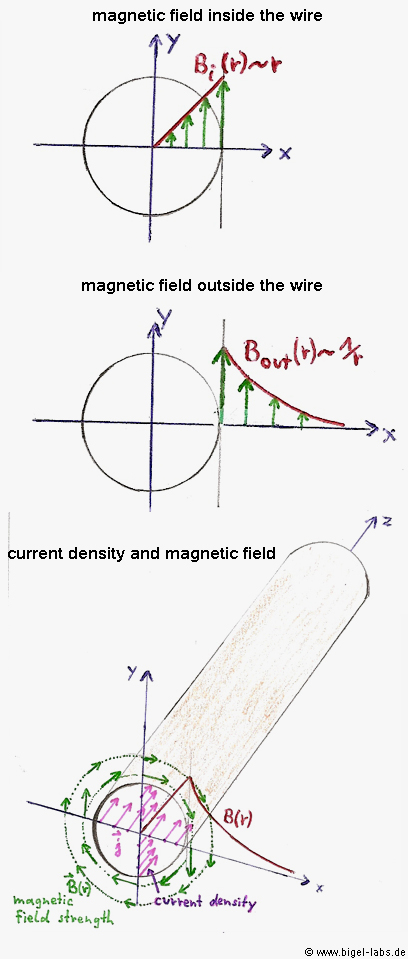
Every conductor has got a inductance depending on diameter,
length, form and material. In general one can distinguish two kinds of
inductance:
The inner inductance and the outside inductance. The
sum of these two is the inductance, which gives us the relation of the
energy created by the currentflow:
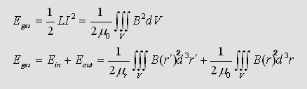
r' are all positions inside the wire
r are all positions uotside the wire
As we now from Biot-Savart the magnetic flux density is
proportional to the current. So, any field vector in the room is created
by all the current densities in the wires. If you want to calculate the
whole magnetic energy in the suround of a wire you could calculate all
the magnetic flux vectors and then integrate over the volume:
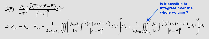
| But isn´t it horrible!?
You would have to integrate over the whole room to get Eout.
This seems to be very difficult. At which distance you could stop
the Inegral. How much energy would be lost far away? There must
exist annother solution to get the energy.... Inductance of a straight wire may be calculated by
using intergration of the field energy density. One can show that
the partial inductance of a wire is equal to [Grover, "Inductance
calculation of coils"].
|
|

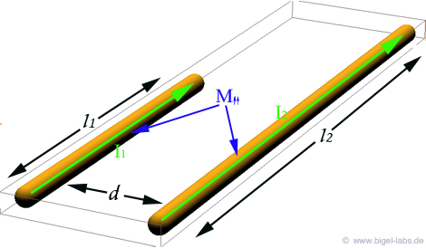
| A parallel wire configuration one can find
in nearly any kind of electronic devices. It´s the simplest
way to transform electric energy from one point to another point.
In experiments with capacitor banks it´s one possible way to
bring the stored energy from the capacitors to the load. For some
experiments it´s ok. But if the goal is to get a huge power
peak, the large inductance of parallel wires will encrease the current
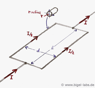
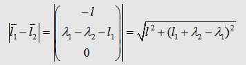
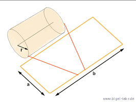
rise time siginficant. So let´s find the inductance we are dealing with in this case: Let´s assume two wires in the form you can see in the following pictures. Between the parts l1 and l2 is a distance of d. . |
|||||||
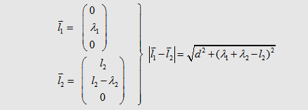
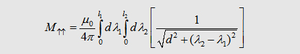
| Mutual
inductance - current in same direction |
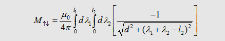
Mutual
inductance - current in opposite direction |
||||||
 |
 |
||||||
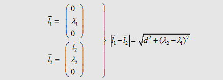
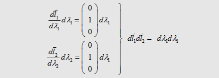
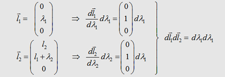
| We can descirbe the
parts l1 and l2 in the
following form with respect to the currents in the wires: |
|||||||
 |
 |
||||||
 |
 |
||||||
 |
 |
||||||
| The integral on the
left and right side can be solved analytical so that we get |
|||||||
 |
|||||||
 |
|||||||
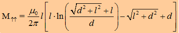
| If we say that l1= l2 we get the the important formula for the mutual inductance of two wires: | |||||||
|
|||||||
|
|
|||||||

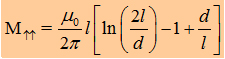

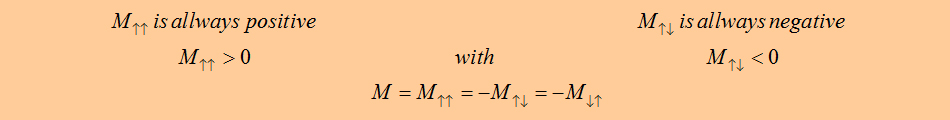
 If
you connect two parallel conductors, the total inductance will decrease.
But what happens there?
If
you connect two parallel conductors, the total inductance will decrease.
But what happens there?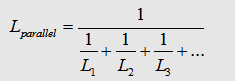
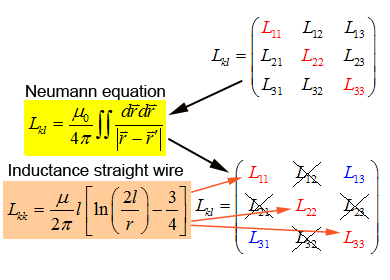
| (Method by using the Neumann-equation) | ||
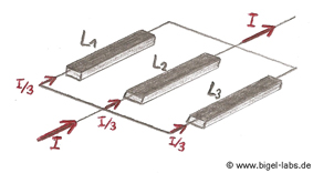
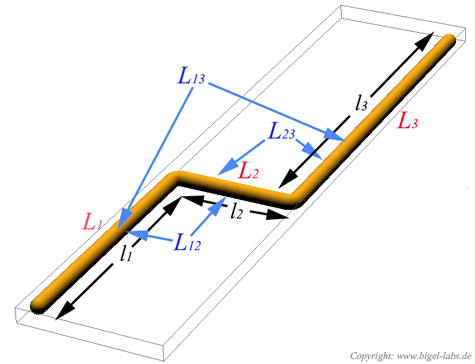
| In every capacitor bank application one can find
inductors in form of steps. If you search for a formula in ingeneer
books to get the Inductance of such a "step wire" you
surely won´t find one. So I tried to get a formula by using
the Neumann-equation. |
||
 |
||
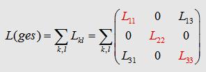
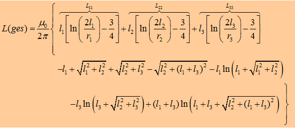
| Inductances
L1,L2,L3
and mutual Inductances L12,L23,L13
of a "step wire"
l1 and l2, l2 and l3 have to be ...... |
||
|
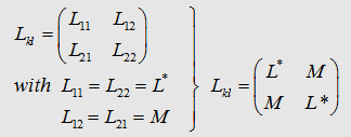
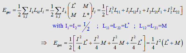
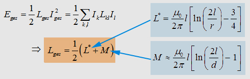
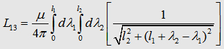
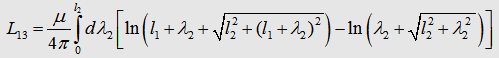
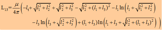
Now, we can write down the the Integral to calculate the matrix
element L13 : The components L12, L21,
L23, L32 of the inductance
matrix become sero, because of the dot product in the Neumann equation. In the table
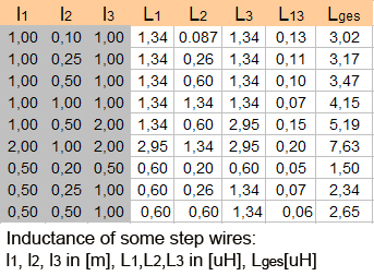
on the right you can watch the inductances of some geometries. As
you may realize the mutual inductance L13
is not that significant. One have to be care of taking L12
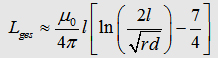
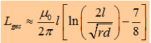
twice in the summation to get Lges. |
||
2.
Inductance of a frame
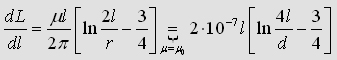
2.1 Calculation with engineer formulas
In many technical
high voltage circles it should be possible to interpolate the wires and
bussbars by geometric forms like: circle, frame, usw..
In the last century many electrical engineers calculated the inductivity
of such forms analytically [Neuman equation] the or by using
finite elements methods [volume integration methods]. After getting the
results they often tried to interpolate the values by special formulas.
One of the greatest engineers was Prof.
Dr. sc. techn. Eugen Philippow. In my opinion his books about theoretical
electrical engineering are one of the bests worldwide. In "Taschenbuch
der Elektrotechnik, Band1" one may find a great inductance formula
for frames which may be calculated analytical [I calculated the Neuman
equation for such a frame and got exactly the same expression ;-)].
|
|
||
 |
 |
|
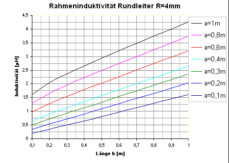
| Diagramm1:
Inductance of frames up to a lenght of 1m |
Diagramm2:
Inductance of frames up to a lenght of 5 m |
|
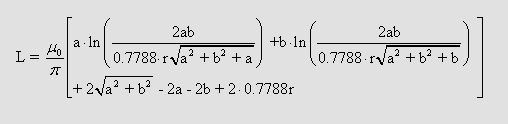 (3.1)
(3.1)2.2
Experimental measurements of Inductnace
With (3.1) it´s quite easy to calculate the inductance of specific
frames. But what about the real value? Is the formula really good enough
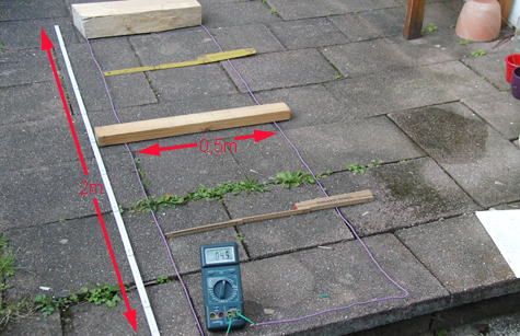
to calculate the real nductance. To get an answer I made some measurements
with a 2,8mm diameter copper-wire:
 |
 |
| Inductance
measurement of a frame: Different sizes of a wireframe were formed. With an LCR-meter the inductance of any frame was captured. Step by step the length b was cutted (each time around 25cm+/-1cm. |
Inductance
of a frame: |
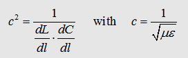
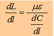
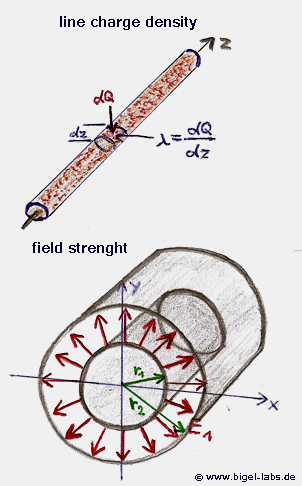
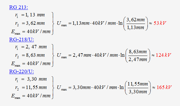
3. Low Inductance Dicharge Circles with high voltage high current Coaxial Cables
In some
Pulsed Power Applications/Experiments any small inducantance of bussbars
etc. could become a problem. If the goal is to get the maximum current
rise time there are several parameters which could be changed:
1.) Higher voltages with smaller capacitance applications could subsitute
applications with low coltage and high capacitance values.
2.) All bussbars and wires should be placed in regard to get as low inductance
as possible.
3.) Substitution of the load supply lines by high voltage coaxial cables
Here I only want to discuss the use of high voltage coaxial cables instead
of the typical used frame lines described before.
Normally coaxial cabels are used in high frequency technology to transport
electromagnetic waves. For pulsed power capacitor banks the transportation
of electromagnetic waves is not so important, because of the relative
low frequencies (around several 10kHz) while the pulses. It´s quite
clear that the lenght of the wires normally used in such experiments are
much much longer than the wave lenghts (around 30km!!) calculated with
l=c/f.
But never the less coaxial cabels are very interesting for pulsed power
experiments. The reason is very simple:
Coaxial cabels have got the minimal Inductance compared with all other
kinds of load supply lines (like a frame)!
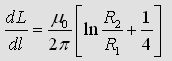
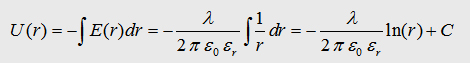
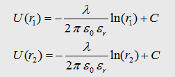
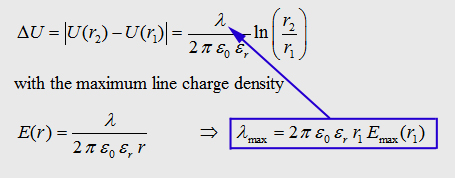
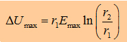
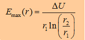
If you calulate the energy inside R1, R2
and R3 you will get the exact formula of
the whole partial inductance of a coaxial cable:
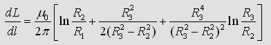 (1.1)
(1.1)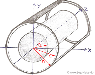
 (1.2)
(1.2) 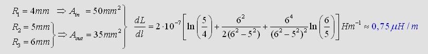
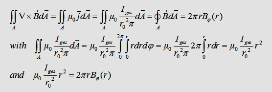
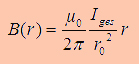
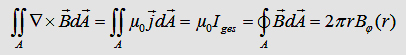
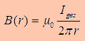
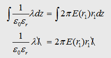
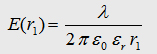
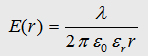
 With
the maxwell eqation and the Gauß law we can write:
With
the maxwell eqation and the Gauß law we can write: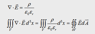

4.
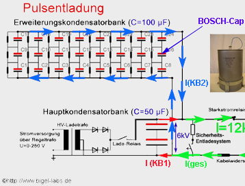
Discharge behavior of the capacitor bank KB1-KB2
4.1 Selfinductance of the used parts
Before I described the methods to calculate the inductance
matrix for parallel wires, step wires and frames. In may capacitor banks
KB1, KB2 one can find many different wires and cabels. To get the inductance
matrix of the whole setup one would have to calculate a 20*20 matrix by
hand. This would take too much time. So I decided to build a programm
which can calculate the inductance matrix with a certain algorithm. The
program is able to combine a set of points [P1(x1/y1/z1),
P2 (x2,y2,y2),
P3 (x2, y2,
z3),...., Pn(xn,
yn, zn)] with lines with a
defined radius r12, r23,
r34,.... r(n-1)n.
At first I had to define the positions of the cables. So it´s easy
possible to calculate the inductance matrix including all the mutual inductances.
By defining different materials (Cu, Al, Fe) and diameters the programm
may calculate the whole inductance and resistance of the system.
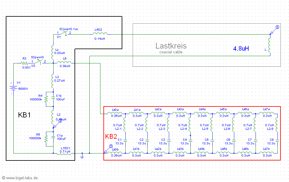
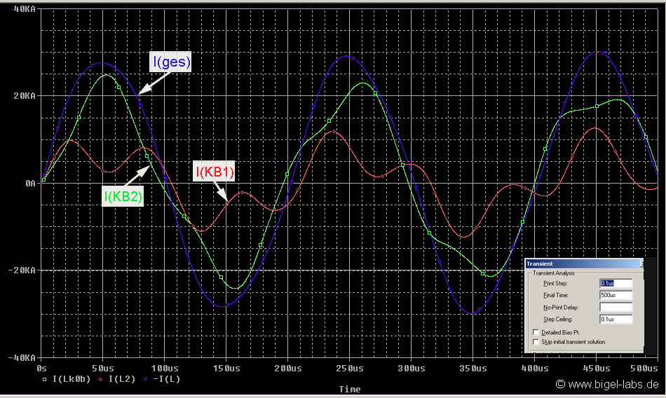
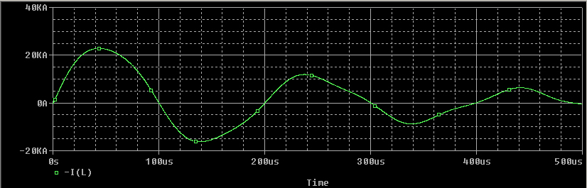
4.2 Current distribution of KB1-KB2
| Current
measurements of the capacitor bank KB1-KB2 usually gives graphs
similar to the
green line. But
what is the current of KB1 and KB2? KB1 has got a capacitance around
50uF, KB2 around 100uF. Are the currents splitted up with the samel
relation 1:2 as the capacitance does? |
|
|
 |
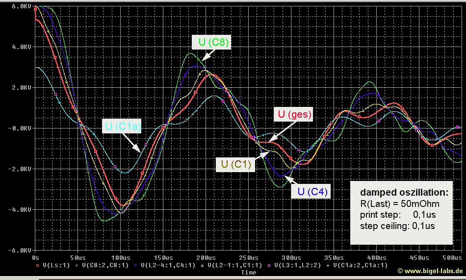
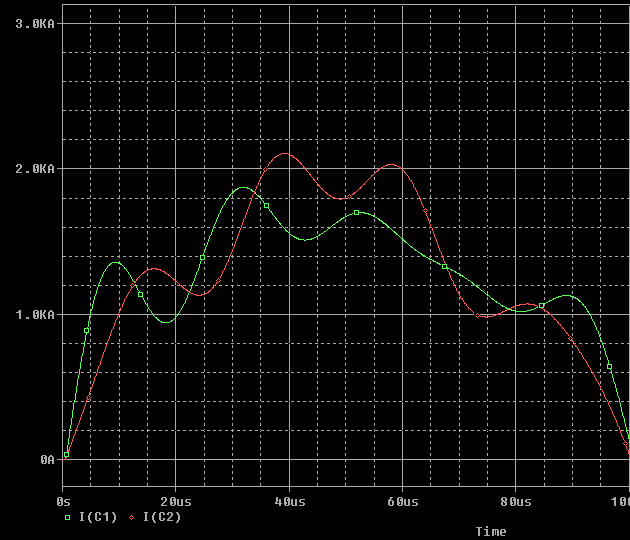
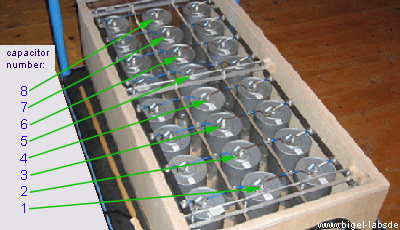
4.3 Current distribution inside KB2
|
The plotts on
the right show the specific currents of the Capacitors C1-C8. One
can find following characteristics:
-
The last capacitor C8 has got not the highest peak current |
 |
||||||||||||||||
|
|
4.4 Simulation of KB1-KB2 and Frequency Analysis with different inductivity
loads
By
analyzing different discharges of the capacitor bank KB1-KB2 with
several load inductances it was possible to figure out a specific
resonance frequency.With Fourieranalsysis within the first two periods
it´s quite simple to find the "middle period lenght"
in this time. By using the Thomson equation  (2.)
(2.)one can find a specific inductance, which represents the CLR-System KB1-KB2.
* Subst. Inductance is the Inductance calculated with equ. (2.) * Inductance inside is the representing the bussbars etc. inside KB1-KB2 without load inductance The graphs on the right show the real discharge currents and voltages of KB1-KB2 as well as the Discharge behavior of the Substitution CLR-circle. |
 |
|||||||||||||||||||||||
|
|
||||||||||||||||||||||||
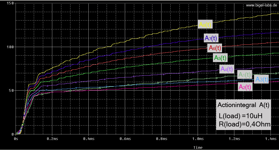
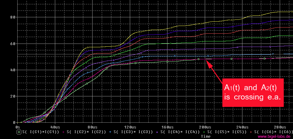
Action Integral Simulations
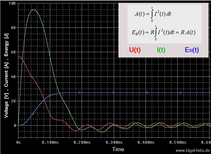
|
|
|
On the right you can watch the results of action integral simulations [also check out this side]. It´s quite interesting that the last capacitor has to withstand around the douple Action value than the second capacitor. The individual capacitors have got a totaly different stress!! |
|
.jpg)
5.
Discharge Simulation of a Capacitor Banks with a Sparc Gap Switch
5.1
Toepler´s sparc gap equations
 Pulsed
power applications with capacitor banks as energy source can be discharged
with different kind of switches:
Pulsed
power applications with capacitor banks as energy source can be discharged
with different kind of switches:
- Sparc gaps
- Mechanical switch
- Ignitrons
- Thyratrons
- Thyristors
- IGBT`s
A traditional sparc gap switch seems to be a very old fashion. But it´s
realy not a bad choise. Ignitrons are filled with huge amounds of mercury
(around 25-100ml). Thyratrons, Thyristors and IGBT`s are hard to get and
do cost a lot of money. A sparc gap is a very strange thing. In the first
nanoseconds the resistance is very large. But after building a plasma
channel between the two electrodes, the sparc resistance is dropping down
very fast depending on the charge flow which went throw the gap.
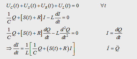
To understand
this phenomena let´s assume a cpacitor discharge circle with the
following parts:
High voltage storage capacitor (capacitance C),
Sparc Gap (resistance RSG(t)),
cable inductance L and a resistance
R.
Without the Sparc
Gap resistance RSG(t)
the discharge circle would oscillate without losing energy in this switch.
All the energy stored in the capacitor would be transfered to the resistor
R, which would become hot. But with a sparc gap, we also
have to think about the resistance RSG(t).
The
capacitor is charged up to several kilovolts (storage energy around some
kJ). While closing the spark gap switch a sparc between a
and b will cause a plasma. If we assume no recombination
of the created ions and electrons, the resistance will drop down, because
of the charged particles in the plasma. Maximilian Toepler found
a formula which describes thris relations in an easy way:
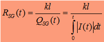
|
Toeplersches
Funkengesetz |
If you
think about formula (1) it´s clear that it´s not possible
to use this formula in numeric simualtions. At the time t=0 one will get
a resistance which is infinity:
![]()
If you would
implement formula (1) in a simulation, the current never could crow up,
which does not represent the reality. With a small modification it´s
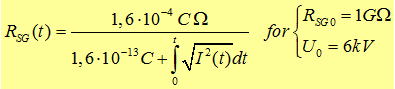
possible to use formula (1). Let´s set the boundary condition that
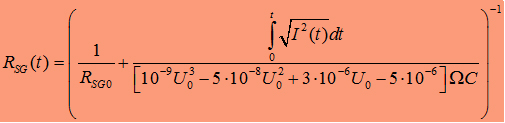
R0=1GO, U0=6kV, l=0,2cm. if we assume a small start charge q0 we get:
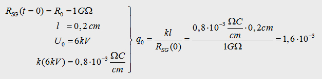
T he value q0 is equal to arround 1 Million free
electrons in the sparc gap switch. So for my simulations of the capacitor
banks KB1, KB2, KB3 I will use the equation
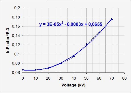
To be moore flexible I tried to interpolate the Graph of k. So it´s
possible to get formulas for any voltage, you want to use in a simulation.
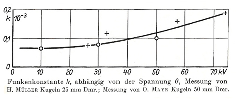
The graph above shows the sparc constant k measured by H.Müller (F.Früngel, Impulstechnik, Erzeugung und Anwendung von Kondensatorentladungen, Technisch-Physiklische Monographien). The graph on the right is fitted with a polynome-function to get a formula whitch describes k(U):
(The voltage is has to be used in [kV], not [V] here) |
|
| Abb.4.1: k-faktor depending on sparc gap voltage |
.jpg) |
.jpg) |
||||||
| Abb.4.2: Brake Down Distance of spherical sparc gaps (spheres 25mm diameter) |
Abb.4.3: Brake Down Voltage of spherical sparc gaps (spheres 25mm diameter) | ||||||
| Abb. 4.2 presents the Discharge Distance of spherical sparc gaps (spheres 25mm diameter) I got from array presented in Impulstechnik, Erzeugung und Anwendung von Kondensatorentladungen. The best fitt I achieved was a third grade polynom in the intervall U=[4kV-45kV]:
If it´s nescesarry to know the maximum break down voltage, one could use this formula:
|
.jpg) |
||||||
| Abb.4.4: f-factor in correlation with sparc gap voltage | |||||||
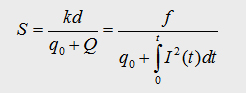
Abb. 4.4 shows the graph of the f-factor, which I defined as the product of k and l:
With this
relation I got a generell modified formula of the sparc gap resistance: 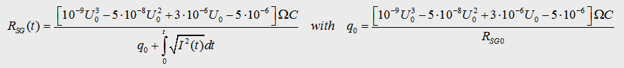 It looks nicer when it´s written as:
|
|||||||
|
|||||||
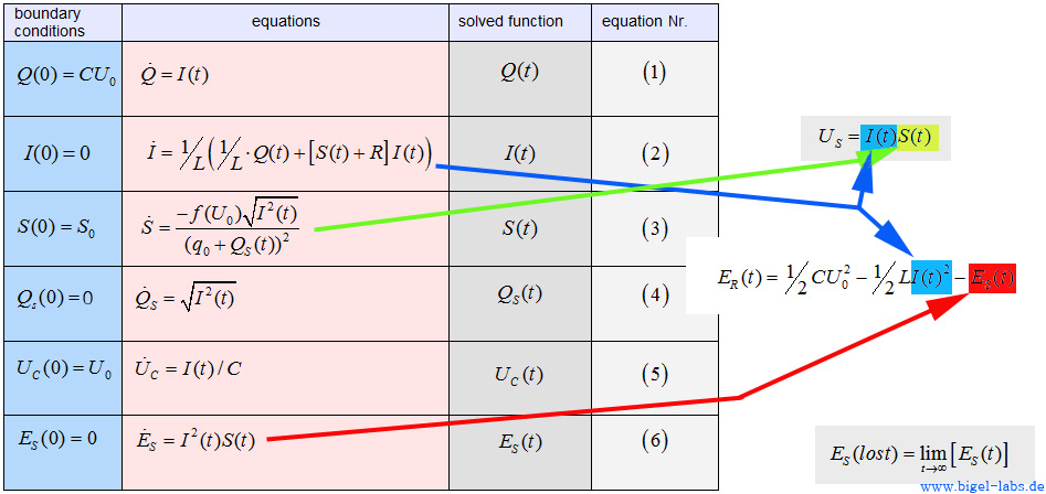
5.2 Coupled Differential equations
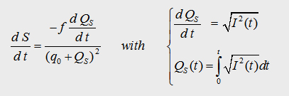
In the following array we can summarise all the founded equations.
5.3 Numerical solutions and simulations

6. Conculsion and Improvements
---->> moore will come soon...........................
last update: October 2012